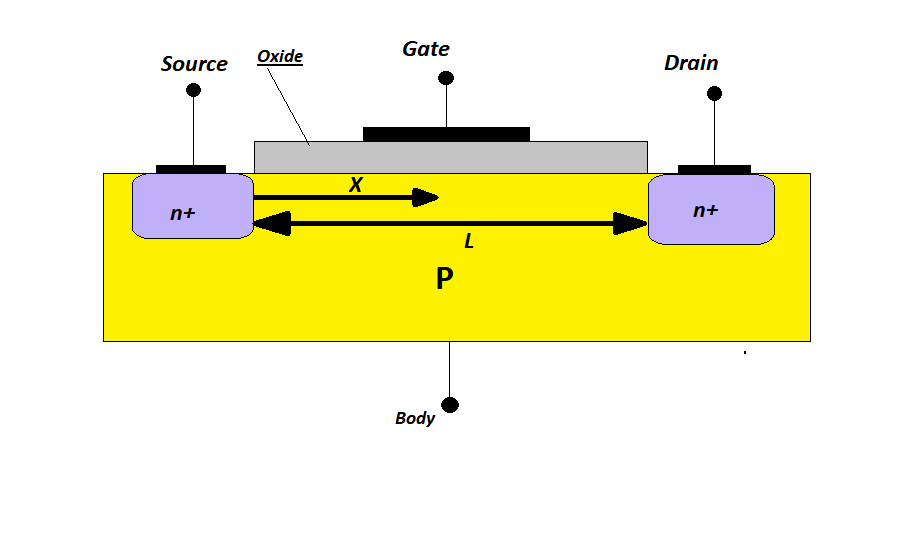
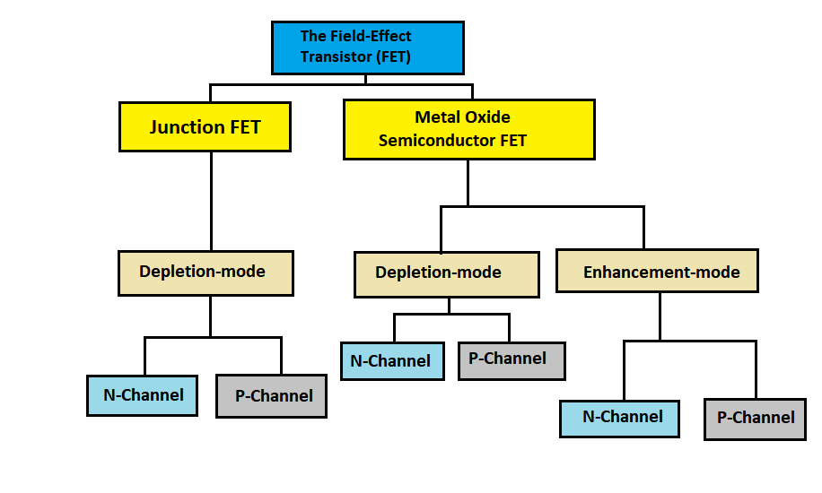
The Field Effect transistors (FET) is a kind of transistor that controls the flow of current in a semiconductor by using an electric field. FETs (also known as JFETs or MOSFETs) are semiconductor devices with three terminals: source, gate, and drain. FETs regulate current flow by applying a voltage to the gate, which changes the conductivity between the drain and source.
The field effect transistor, or FET, is a critical electrical component used in many different fields of the electronics industry.
The FET is utilised in a wide range of circuits made up of discrete electronic components, from RF technology to power regulation and electronic switching to general amplification.
The field effect transistor, or FET, is most commonly used in integrated circuits. In this application, FET circuits consume far less power than ICs based on bipolar transistor technology. This permits the operation of very large scale integrated circuits. If bipolar technology were employed, the power consumption would be orders of magnitude higher, and the produced power would be much too massive to dissipate from the integrated circuit.
Through an electric field, the FET transistor (field-effect transistor) affects the shape and consequently conductivity of the charge carrier in a semiconductor. Because they perform a single-carrier function, FET transistors are also known as unipolar transistors. All FET types have a high input impedance.
A Field Effect Transistor (FET) is a semiconductor device with three terminals. It works by using a regulated input voltage. JFETs and bipolar transistors seem extremely similar. However, the BJT is a current-controlled device, whereas the JFET is voltage-controlled.
There are typically two types of FETs (Field Effect Transistor )available.
Field Effect Transistor Junction (JFET)
Junction FET, JFET: The gate connection of a junction FET, or JFET, is provided by a reverse biassed diode junction. The structure is made up of a semiconductor channel that might be N-type or P-type. The channel is then built with a semiconductor diode such that the voltage on the diode influences the FET channel.
In operation, this is reverse biased, which means it is essentially separated from the channel, with just the diode reverse current flowing between the two. The JFET is the most basic form of FET and was the first to be invented. Nonetheless, it continues to give good service in many sectors of technology.
- Cutoff Region – This is the region where the JFET is turned off, implying that there is no drain current and ID flows from drain to source.
- Ohmic Region – In this region, the JFET begins to exhibit resistance to the drain current, ID, which is beginning to flow from drain to source. The current flowing through the JFET is proportional to the voltage applied.
- Saturation Region – The device is considered to be in the saturation region when the drain-source voltage reaches a value such that the current flowing through the device is constant with the drain-source voltage and fluctuates exclusively with the gate-source voltage.
- Breakdown Region – When the drain to source voltage, VDS, surpasses the maximum threshold value, the depletion area breaks down, the JFET loses its capacity to resist current, and the drain current grows endlessly.
FET Metal Oxide Semiconductor (IGFET)
An insulated layer is used between the gate and the channel in MOSFETs. This is often generated from a layer of semiconductor oxide.
Any form of FET with an insulated gate is referred to as an IGFET. The silicon MOSFET – Metal Oxide Silicon FET – is the most prevalent type of IGFET. The gate is constructed of a metal layer that is laid down on the silicon oxide, which is then on the silicon channel. MOSFETs are widely employed in a variety of electronic applications, notably in integrated circuits.
The IGFET / MOSFET’s major feature is the extremely high gate impedance that these FETs can give. However, there will be an accompanying capacitance, which will lower the input impedance.
- Cutoff Region :The MOSFET remains OFF in the cut-off area because there is no current flow in this region. MOSFETs behave like open switches in this case and are consequently employed when electronic switches are required.
- Ohmic Region: In the Ohmic or linear zone, the drain to source current increases as the voltage across the drain to source increases. MOSFETs can be employed as amplifiers when operated in this range.
- Saturation Region: In this area, the drain to source current value remains constant despite the increase in voltage across the drain to source. This occurs only when the voltage between the drain to the source terminal exceeds the pinch-off voltage.
Field Effect Transistor Junction
The operation of a Junction Field Effect Transistor is solely dependent on the flow of majority carriers (electrons or holes). JFETs are made up of a N type or P type silicon bar with PN junctions on the sides. The following are some key factors to remember regarding FET.

Gate :To make a PN junction, both sides of a N type bar are strongly doped using a diffusion or alloying process. These doped zones are known as gates (G).
Source: The source is the place at which the majority of carriers enter the semiconductor bar.
Drain :The drain is the exit point for most carriers when they leave the semiconductor bar.
Body :The Body is the region of N type material through which the most of carriers flow from source to drain

FETs with n channels
A negative gate-to-source voltage in an n-channel “depletion-mode” device causes a depletion area to increase in width and encroach on the channel from the sides, narrowing the channel. If the active zone grows to entirely shut the channel, the channel resistance from source to drain increases, and the FET is essentially switched off like a switch (see right figure, when there is very small current). This is referred to as “pinch-off,” and the voltage at which it happens is referred to as the “pinch-off voltage.” A positive gate-to-source voltage, on the other hand, expands the channel and allows electrons to flow freely (see right figure, when there is a conduction channel and current is large).
FETs with p-channels
A positive voltage from gate to body in a p-channel “depletion-mode” device extends the depletion layer by driving electrons to the gate-insulator/semiconductor interface, exposing a carrier-free zone of immobile, positively charged acceptor ions.
A conductive area does not exist in a p-channel “enhancement-mode” device, hence negative voltage must be employed to establish a conduction channel.
A thin layer of P type material has been produced on a N type substrate. The crystal structure and schematic symbol of an N-channel JFET are seen in the image below. The gate is built with N type material on top of the P channel. Lead wires are connected at the channel and gate ends. The remainder of the construction specifications are comparable to those of an N-channel JFET.
Normally, the gate terminal is made positive with regard to the source terminal for general functioning. The size of the P-N junction depletion layer is determined by changes in reverse biased gate voltage levels. JFETs can be adjusted between full conduction and cutoff state with a tiny change in gate voltage.
The advantages and disadvantages of FET
In comparison to the bipolar transistor, the FET offers several benefits and downsides. Field-effect transistors are used in low-signal applications such as wireless communications and broadcast receivers. They are also desirable in high impedance circuits and systems. In general, FETs are not employed for high-power amplification, which is necessary in big wireless communications and broadcast transmitters.
On silicon integrated circuit (IC) devices, field-effect transistors are manufactured. A single integrated circuit (IC) can include thousands of FETs as well as resistors, capacitors, and diodes.
Related posts